Test Modes

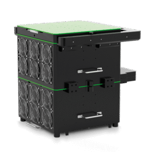
Cosmic test systems validate power semiconductor devices across static, dynamic, thermal, and ruggedness requirements — from incoming inspection through production test and failure analysis.
Static Parameter tests

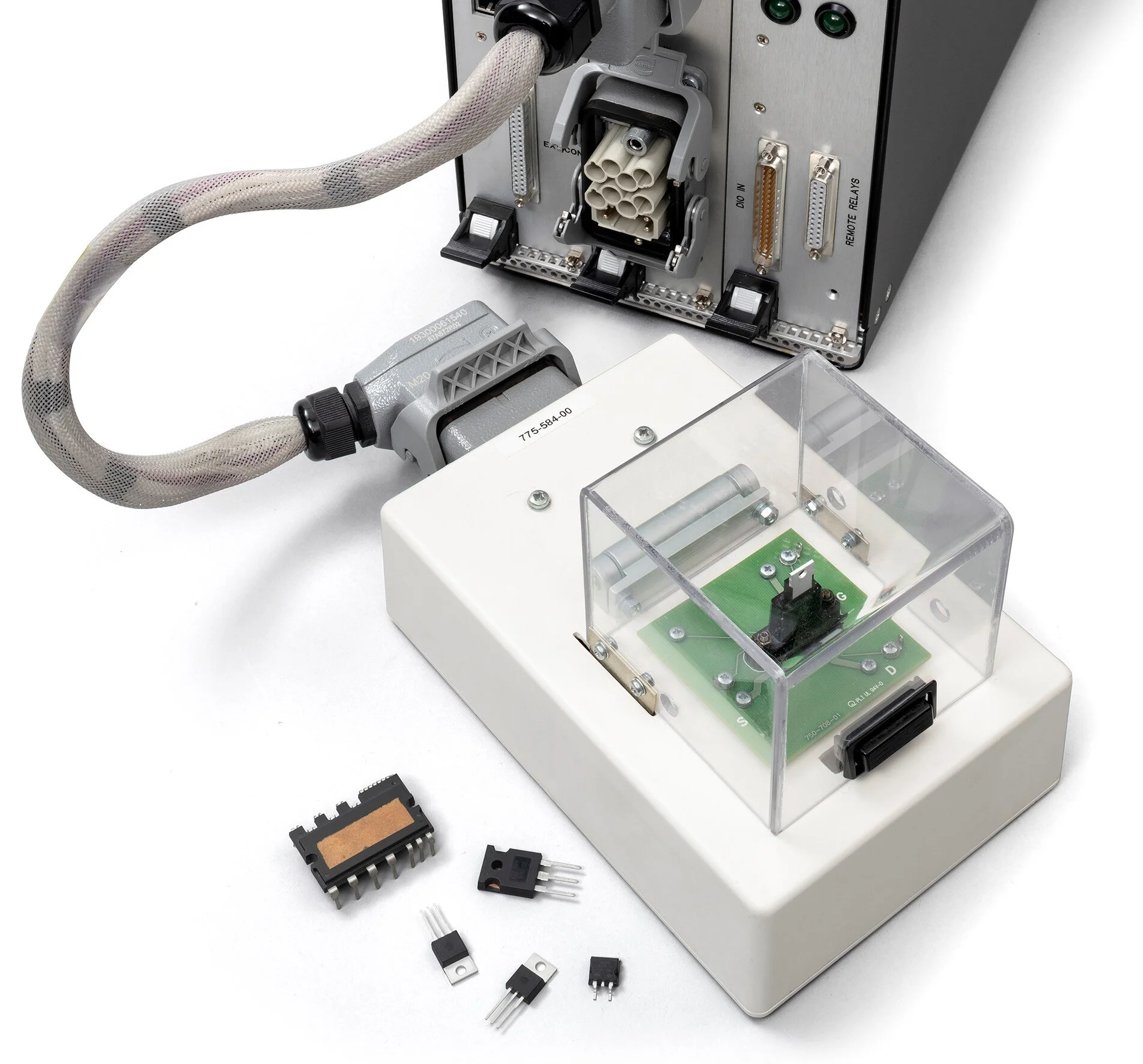
Static power testing evaluates the DC electrical characteristics of semiconductor devices under steady-state operating conditions, determining whether a device meets its datasheet specifications.

Features

Measurement
Test Description
Test Insight
BVDSS
Confirms MOSFET drain-source avalanche withstand at the rated breakdown voltage.
Demonstrates robust blocking margin for high-voltage designs.
BVCES
Validates IGBT collector-emitter breakdown with the gate shorted to emitter.
Proves voltage class and device ruggedness.
IDSS
Quantifies off-state drain leakage under applied drain-source voltage.
Screens leakage paths and oxide-related defects.
IGSS
Measures gate leakage under controlled gate bias.
Highlights gate-oxide integrity for reliable switching.
VGS(th)
Captures MOSFET turn-on threshold from gate voltage to drain-current response.
Supports consistent drive design and device binning.
RDS(on)
Measures enhanced-state drain-source resistance at defined gate bias.
Shows low-loss conduction and efficiency potential.
VCE(sat)
Measures IGBT collector-emitter saturation drop during conduction.
Benchmarks conduction efficiency and thermal performance.
VF
Checks diode or body-diode forward voltage at specified current.
Confirms predictable freewheel and rectification behaviour.
ICES
Measures IGBT collector-emitter leakage with the gate grounded.
Verifies low standby loss and blocking reliability.
IGES
Measures IGBT gate-emitter leakage under gate bias.
Assures gate insulation quality and long-term robustness.
Transfer Char.
Maps current versus gate voltage to reveal transconductance.
Supports drive optimisation and product positioning.
Output Char.
Sweeps output current versus drain or collector voltage across operating regions.
Reveals safe operating behaviour and application fit.

Gate Resistance & Capacitance

Accurate measurement of MOS gate resistance and capacitance.

Features

Measurement
Test Description
Test Insight
Rg (Gate resistance)
Measures the effective resistance between the gate terminal and the internal gate structure using an AC signal.
Characterises switching behaviour and gate drive requirements.
Cg (Gate Capacitance)
Measures the total capacitance seen at the gate terminal.
Characterizes switching behavior and gate drive requirements.
RgBias
Applies programmable DC gate or drain bias during measurement.
Evaluates gate characteristics under different bias conditions.

Dynamic Switching tests

Dynamic testing characterizes semiconductor behavior during switching events under realistic operating conditions — essential for EVs, renewable energy systems, motor drives, and industrial power supplies.

Test Methods

  • Single Pulse
  • Double Pulse
  • Clamped Inductive Load
  • Diode Recovery
  • Short Circuit
  • Dynamic Reverse Bias (DRB)

Reason Why

Fast characterization

Full dynamic characterisation in under 200 ms.

Low inductance test head

Compact, remote head for hard-dock handler mounting.

1 ns waveform capture

On-screen switching waveforms at production speed.

Features

Measurement
Test Description
Test Insight
td(on)
Time between the gate signal and the start of current conduction.
Shows fast turn-on response for efficient converters.
td(off)
Time between gate removal and current decay.
upports responsive, predictable switching control.
tr
Tracks how quickly current or voltage transitions upward.
Highlights high-speed switching capability.
tf
Tracks downward current or voltage transition during turn-off.
Confirms clean turn-off with lower switching loss.
EON
Quantifies turn-on energy loss under defined pulse conditions.
Enables efficiency benchmarking and loss modelling.
EOFF
Quantifies energy lost during device turn-off.
Helps optimise thermal budget and converter efficiency.
QG
Total gate charge required to fully switch the device.
Guides gate-driver sizing and power design.
QGD
Miller plateau charge during the device voltage transition.
Reveals switching behaviour and drive requirements.
QRR
Reverse-recovery charge removed after diode conduction.
Reduces switching loss, device stress, and EMI risk.
trr
Time required for diode recovery after reverse bias.
Supports high-frequency converter validation.
IRRM
Peak reverse-recovery current following diode conduction.
Assesses recovery stress and ruggedness.
Double Pulse
Two-pulse method that recreates real switching events.
Characterises losses under application-like conditions.
Short Circuit
Controlled fault test measuring short-circuit withstand.
Validates ruggedness and protection strategy.
DRB
Evaluates reverse-biased switching under dynamic stress.
Assess robustness in power converters.

DRB testing is an essential reliability qualification for wide bandgap semiconductors such as SiC MOSFETs and GaN HEMTs. It applies high-voltage switching conditions under reverse bias to replicate real-world power electronics stress, helping manufacturers evaluate long-term reliability, detect gate-oxide or body-diode weaknesses, accelerate lifetime testing, and qualify devices to automotive and industrial standards.

Thermal tests

Thermal testing determines how efficiently heat is transferred from the semiconductor junction through the package to the external environment — essential for evaluating package integrity, die attach quality, and long-term reliability. Transient thermal analysis reveals internal package construction without destructive inspection.

Features

Measurement
Test Description
Test Insight
RθJA
Measures junction-to-ambient resistance across the full thermal path.
Predicts operating temperature in real-world cooling conditions.
ΔVSD Method
Uses the diode forward-voltage shift (ΔVSD) to estimate junction temperature non-invasively during testing.
Enables non-invasive thermal measurement during production test.
ΔVDS
Tracks drain-source voltage shift as a proxy for internal thermal resistance.
Gives proof of superior mechanical packaging and die-attach quality.
ΔVTH Method
Measures shifts in gate threshold voltage (Vth) to evaluate semiconductor degradation, stress wear, and thermal performance.
Detects permanent or temporary changes in the gate-to-source voltage needed to start channel conduction.

Avalanche & ruggedness tests

Avalanche testing evaluates the capability of a power semiconductor to safely absorb inductive energy during switching events without catastrophic failure — simulating conditions in motor drives, automotive electronics, and inductive switching applications.

Features

Measurement
Test Description
Test Insight
UIS
Tests device survival during unclamped inductive switching events.
Verify avalanche ruggedness.
UIL
Evaluates switching under inductive load conditions.
Simulate real application stress.
EAS
Measures the avalanche energy absorbed before failure.
Determine energy capability.
Repetitive UIS
Repeats avalanche events to assess long-term durability.
Evaluate lifetime robustness.
Avalanche I
Measures current flowing during avalanche breakdown.
Characterise breakdown behaviour.
Avalanche V
Records voltage reached during avalanche operation.
Confirm breakdown performance.

Get in touch